SPRINT-CAD:
Industrial-Networked TCAD Using Shared Parallel Computers
The SPRINT-CAD project will bridge the capabilities of solid modeling, FEM-based parallel computation of fabrication processes and electrical analysis of the resulting IC structures. Under an integrated information model, computational prototyping will be provided for complete circuit blocks across the levels from circuit performance through the underlying fabrication technology. Models to represent etching, deposition, oxidation, diffusion and stress analysis from process steps that are necessary in the creation of electrical devices will be developed. The focus is however not on developing yet another point tool, but on creating a computational prototyping environment that can accommodate new and existing physical models and numerical methods, as well as eliminate the interface barriers in communication and abstraction between different levels of tools. The software maintainability and configurability are derived from object-oriented design, and large computational requirements are tackled by intelligent abstraction and parallel programming. This next-generation TCAD environment is designed to strongly link to and interact with the manufacturing process and therein provide system designers with practical methods to prototype, examine and conceptualize the underlying physical properties of new technology. Better tradeoff decisions in a timely manner are projected with the fast moving semiconductor technology base.
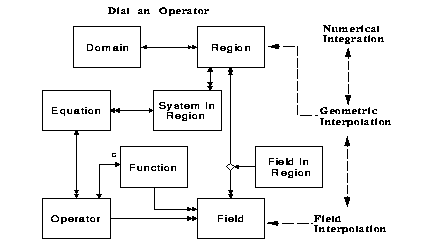
To accurately simulate modern semiconductor process steps, TCAD tools must include a variety of physical models and numerical methods. Increasingly complex physical formulations are required to account for effects that were not important in previous generations of technology. As a specific example, the impurity diffusion mechanisms owing to point defects and damage kinetics are not well understood, and thus flexibility in definition of models is highly desirable. An object-oriented approach has been applied to implementing a 1-2-3D finite-element dial-an-operator PDE solver, which is named as ALAMODE (A LAyered MOdel Development Environment). The control interface is based on Tcl and allows layered access to model definitions and solution techniques.
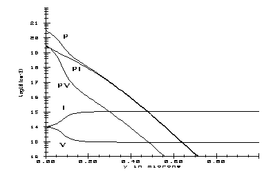
As an example, we solve a system of five reactive-diffusive equations for phosphorus diffusion. This five-species model contains the diffusion, recombination and kinetic reaction of phosphorous, interstitial, vacancy, Pairs of phosphorous-interstitial and phosphorous-vacancy. The profiles developed during a 10 minute, 900C anneal are shown below. Multi-species reactive-diffusive systems, similar to the one shown, are becoming increasing important to model low temperature and rapid thermal annealing as well as implant damage enhanced diffusion.
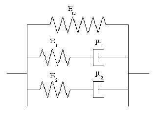
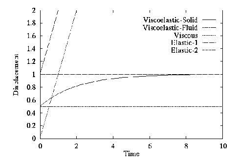
The constitutive modeling of oxidation is important for predicting both the shape and the stress of structures routinely created in IC processes. The linear elastic model will predict unrealistic stress (up to 1.5e11 dynes/cm2 in cylinder oxidation. At these stresses SiO2 is known to develop gross mechanical defects. But no such defects were observed in experiment, since stress can be relaxed by deformation in SiO2. The linear viscous model also fails to replicate the initial elastic behavior of oxidation and overestimates the stresses for low-temperature oxidation. For the SprintCAD efforts, we have chosen the viscoelastic constitutive model with finite deformation in the finite-element discretization, which is more generally applicable. Our preliminary results for the 1D viscoelastic model are shown below. This model will be tested both under FEAP and ALAMODE/SUPREM OO7 implementations.
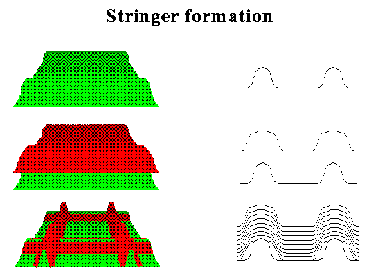
Physical modeling of etching/deposition based on Hamilton-Jacobi equations has been demonstrated in 2D SPEEDIE. The surface evolution based on the string model has been connected to the server-based SUPREM OO7 architecture. A minimal SWR specification (full documentation) for the surface mesh server has been defined from our experience with an integrated example containing all process modeling steps. Modeling of 2D anisotropic etch for deep trench technology has been successfully demonstrated. The movie of moving boundary due to etch/depo through FOREST/SPEEDIE interaction has been generated. Calibration with SEM measurements has been performed to determine various parameters (such as sticking coefficients).
The 3D etch/depo simulation using the physical models in SPEEDIE is now under way. We will use the stringer problem as an example. The 3D surface mesh and visualization is temporarily based on the Berkeley SAMPLE3D Lithography Tool. As an example, to prevent undercut in thin metal interconnect lines, more careful control of etch time is necessary. However, this produces stringer problems at crossover points. To model this phenomenon accurately, physical etching models in SPEEDIE will be extended to 3D.
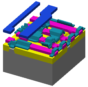
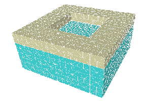
Solid geometry modeling can provide essential communication between volume-mesh-based and surface-mesh-based simulation tools based on a consistent geometry representation. Also, by various geometry manipulations, it can quickly prototype 3D structures when only 1D and 2D simulation or measurement results are available for specific conditions. The geometry modeling utility has been implemented using the ACIS geometry engine and can be accessed through a new minimal SWR (full documentation) (Semiconductor Wafer Representation) specification. The 3D geometry utility has been connected with the FOREST 2D field server, the CAMINO 3D gridder, diffusion and oxidation capabilities (SUPREM) as well as etching and deposition (SPEEDIE) tools. A 3D example of via by CAMINO with multi-region capability (silicon and oxide) is shown below. For efficient device simulation, the anisotropic weighting for oct-tree based meshing has been implemented using heuristic rules.
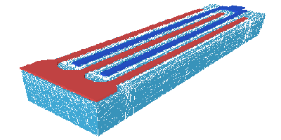
A solid geometry modeling tool (VIP-3D) has been utilized to prototype a commercial wireless communication BJT. This is a first-time demonstration of the ability to go directly from IC process and mask specifications to extraction of RF distortion. Using IC layout-based specification of this complex RF bipolar transistor, including both 3D and 2D computational models of the device, a new harmonic balance (HB) simulator directly supports the analysis and extraction of exactly which regions in the device contribute to harmonic and IM distortion. This new computational approach now allows the circuit designer and the IC technologist to communicate directly and unambiguously about the trade-offs being made in development of new structures for RF and other wireless applications. As an example, the Stanford team demonstrated the extraction of distortion for a 1.5 GHz bipolar within a cellular phone application. The IM tones can now directly be correlated with internal device effects such as collector and base doping parameters, thereby setting the stage for optimizations that will improve overall system performance.
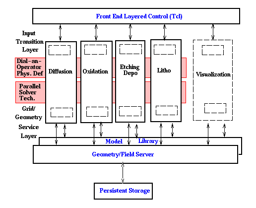
With the minimal SWR specification discussed in the previous section as the procedural interface for geometry/field server, to achieve a configurable and reusable TCAD framework, we have further analyzed process simulation information flow carefully and separated other common functionalities such as the parameter/model library and the visualization tools from the physical definition and numerical solvers. In this open framework named as SUPREM OO7 (agent-based heterogeneous tool integration architecture), one can choose to use individual tools and any combination. For example, one has the choice of using SUPREM-IV diffusion code or the new dial-an-operator solver imbedded in ALAMODE for impurity diffusion simulation. All tools communicate wafer representation through the geometry/field servers, and additional information for individual tools such as model and boundary condition setup can come from either the model library or the front-end controller.
The finite element derivative is discontinuous across the inter-element boundaries. To obtain acceptable results for derivatives, resort is generally made to a nodal averaging or projection process. The smoothed derivative can serve as an approximation to the derivative of the exact solution and the error can be estimated by the difference of the smoothed and the finite element derivatives. We have implemented the projection estimate and Zienkiewicz-Zhu estimate.
Last Revision: 1/27/96