Another challenges for physical prototyping systems are from the computational resources. The present environment for using TCAD commercially is dominantly based on engineering workstations (EWS) and is thus practically limited to two-dimensional (2D) simplifications of the actual design problems---neither the methodology nor the computer resources are in place to address the more complete problems which are inherently three-dimensional (3D) such as stress-induced defects. TCAD tools for large-domain 3D problems need to exploit the parallel computing capabilities that are generally applicable to both high performance computing (HPC) stations such as IBM/SP systems and EWS connected by efficient networking.
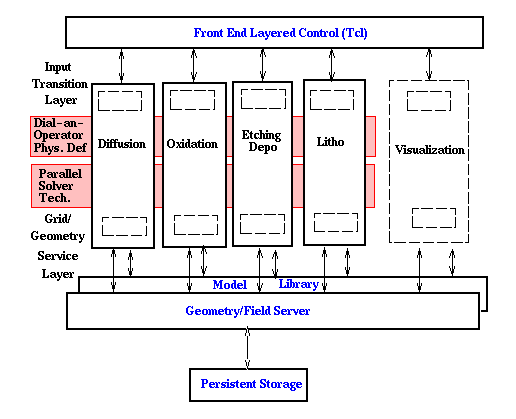
The SPRINT-CAD project bridges the capabilities of solid modeling, FEM-based parallel computation of fabrication processes and electrical analysis of the resulting IC structures. Under an integrated information model, an enabling "computational engine" for technology prototyping is being developed, which can handle complete circuit blocks across the levels from circuit performance through the underlying fabrication processes. Models to represent etching, deposition, oxidation, diffusion and stress analysis from process steps that are necessary in the creation of electrical devices are also being developed. The focus is however not on developing yet another point tool, but on creating a computational prototyping environment that can accommodate new and existing physical models and numerical methods, as well as eliminate the interface barriers in communication and abstraction between different levels of tools. The software maintainability and configurability are derived from object-oriented (OO) design, and large computational requirements are tackled by intelligent abstraction and parallel programming. This next-generation TCAD environment is designed to strongly link to and interact with the manufacturing process and therein provide system designers with practical methods to prototype, examine and conceptualize the underlying physical properties of new technology. Better trade-off decisions in a timely manner are projected with the fast moving semiconductor technology base.
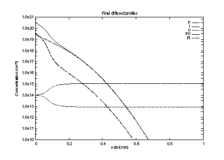
As an example, we solve a system of five reactive-diffusive equations for phosphorus diffusion [5]. This five-species model contains the diffusion, recombination and kinetic reaction of phosphorous, interstitial, vacancy, pairs of phosphorous-interstitial and phosphorous-vacancy. The profiles developed during a 10 minute, 900�C anneal are shown below. Multi-species reactive-diffusive systems, similar to the one shown, are becoming increasing important to model low temperature and rapid thermal annealing as well as implant damage enhanced diffusion. The physical model can be completely described in a simple TCL script, which is explained in detail in Appendix A. The results are shown in Figure 3 and have been compared favorably with the 1D PEPPER diffusion simulation tool. Other examples include boron segregation (benchmarked with SUPREM IV), 1D and 2D SUPREM mesh and 3D FLOOPS mesh, and diffusion in poly-silicon by considering the average grain boundary growth/recombination. Another example of ALAMODE is demonstrated for boron diffusion [6]. The new boron model includes reactions of point defects and defect-dopant pairs, considering their charge states, and the dopant inactivation by the introduction of a boron clustering reaction. The six transport equations and complex constitutive models for diffusive and reactive terms have been completely described in the TCL extension language without any modification and compilation of the source code. Rate of convergence and level of accuracy are comparable to the original implementation for the specific model.
In the dial-an-operator regime, since the stiffness of the coupled system of equations is determined by the user, numerical stability of the simulation demands more robust time stepping and nonlinear iterative schemes. Although it is unlikely to have a universal solution for all types of PDEs, the reactive-diffusive systems can be reasonably treated with TR-BDF2 time discretization and nonlinear convergence validation heuristics. To further accelerate convergence rate in the initial phase of nonlinear Newton iterations, damped Newton methods with different line search schemes are implemented to avoid numerical overshoot. For the new physical models defined in ALAMODE, the Jacobian matrix may be very stiff, such as in the case of the five-species model where dopants and dopant-defect pairs have very different scales of transport coefficients, and the damped Newton scheme can help the overall convergence of the numerical system. A hierarchy of spatial error estimators, including implicit/explicit and inter-/intra-element methods, are formulated and partially connected to ALAMODE. Error fields for explicit inter-/intra-element contributions are verified for the diffusion equation. Time domain error estimation for general trapezoidal schemes including local and global discretization errors has also been formulated. The local truncation error is based on the divided difference approximation and the global error is calculated using the mass and Jacobian matrices in the nonlinear iteration. The formulation is tested against the standard van der Pol equation for nonlinear systems. The conventional constant-step backward Euler method, although stable and convergent, is not only less efficient owing to unnecessary fine steps in slow transient regions, but also heavily polluted by global errors and hence very inaccurate after a fast transient region. Along with the error estimator implementation, access to strong forms of operators are built, which will later be extended to Galerkin-Least-Square (GLS) implementation.
For validation of the physical models and boundary movement algorithms, a wide range of processes including Low Pressure Chemical Vapor Deposition (LPCVD), Atmospheric Pressure Chemical Vapor Deposition (APCVD), Plasma Enhanced Chemical Vapor Deposition (PECVD), Physical Vapor Deposition (PVD), and Self-Aligned Contacts (SAC) are calibrated by matching with the 2D cross section of the SEM pictures, and stringer formation by qualitatively comparing the 3D SEM pictures. Elimination of non-physical, rule-base boundary movement has made calibration much easier since numerical errors can be better controlled. Important physical features, such as polymer accumulation in High Density Plasma Oxide Etching (HDPOE) and facet formation in the sputtering etchback, are successfully demonstrated within the new SPEEDIE.
High Density Plasma (HDP) processing has many advantages for anisotropic dry etching and air-bridge dielectric deposition on high aspect ratio structures. However, its modeling involves many mechanisms that cause both etching and deposition depending on the ion distribution, sputtering probability and source viewing angles. For boundary movement schemes, it is very hard to employ rule-based algorithms on discontinuously bent edges for degenerate conditions, since neighboring segments may flip sign in boundary velocity. The level-set method can be easily extended for modeling HDP systems, since simultaneous etching/deposition can be explicitly accounted for in the Hamilton-Jacobi equation of the level set function.
Calibration of etching and deposition simulation on 3D problems are very difficult and not commonly seen in the literature, not only because 3D simulation tools are much more computationally expensive and not widely available, but also because 3D profile characterization methodologies are limited by insufficient accuracy in positioning 2D cross-section measurements. An L-shaped test structure is chosen to overcome this characterization difficulty by 45-degree angle cuts at various positions. 3D simulation is performed using the physical models in SPEEDIE, whose parameters are calibrated using 2D infinite-width trench simulation, and the level-set method, which can accurately and robustly model complex 3D boundary movement. 3D effects such as the flattening and thinning of the bottom coverage going into the corners can be clearly observed in both measurement and simulation. Also, good match between various 2D SEM and simulation cross sections show the physical model and the boundary movement method are accurate in 3D. The detailed comparison is shown in Appendix B. This is an important starting point for genuine 3D analyses on more complex structures.
For the level-set method, since volume grid instead of surface grid is used, computational efficiency has been a concern even if adaptivity is used. Efficiency benchmarks on etching/deposition simulation have been established for various physical models and staggering schemes. The most CPU intensive part is at the transformation between boundary representation, which is required only if re-emission or surface diffusion is included. However, the solution of the large linear systems of equations dominate the entire simulation when those models are included, and hence the computational penalty using the level set method is not significant.
Introduction of the Eulerian representation of the interface (such as the previous level-set method) will require either frequent transformation between boundary types or posing interface conditions such as segregation directly on the Eulerian grid. However, the Eulerian representation offers several attractive features including simple gridding, robust boundary movement and accurate curvature estimation. These advantages are critical for efficient oxidation simulation, but transformation between boundary types are impractical since the diffusion equation is solved at every time step. Although element base functions can be extended to high orders to improve accuracy, the conventional finite-element method can hardly follow discontinuous fields within the element without employing expensive shock-tracking methods. Also, the physical origin of segregation arises from variation of the chemical affinity in different materials, and is not similar to the shock formation mechanism in hydrodynamics which requires the source velocity equal to the front velocity. Finite-element base functions employing steps represented with delta functions as their derivatives have been developed. Together with the level-set boundary representation, the interface conformity constraint on volume grids is eliminated for modeling segregation effects. The detailed formulation and proof of convergence is documented in Appendix C.
It is established that the waveform relaxation technique is stable and efficient for large sets of ordinary differential equation (ODE) systems as in circuit simulation. Parallelization based on waveform relaxation is attractive since the calculation on subsystems can be asynchronous. Application of waveform relaxation for partial differential equations (PDE) with subsystems partitioned by domain decomposition with controllable overlap regions is very promising for parallelization of the reactive-diffusive systems, since stability and rate of convergence are directly related to the maximum principle (the ordering principle if the reactive term is strong). This will be continuously investigated in the follow-on PARASCOPE project.
For the next decade, it is still expected that many algorithmic improvements on numerical methods and computational geometry for 3D problems will be proposed. An open environment for plug-in new gridding algorithms is necessary for server longevity. Under the SprintCAD project, we have taken a hybrid direction to take advantage of the previous two approaches. A minimalistic SWR is defined with sufficient access and functionality, but only the global access method is specified (similar to Berkeley SPARSE package), not the class. The complete applicational procedural interface (API) is listed in Appendix E. It is much easier for existing gridders and tools to write socket procedural interfaces to conform to the minimal SWR 0.3 specification, while there are still a rich set of functionalities, including conformal gridding, boundary movement and smoothing, adaptation to an error field and consistent field storage. Coarse-grain parallelization of the SWR is under continuous study in the follow-on PARASCOPE project.
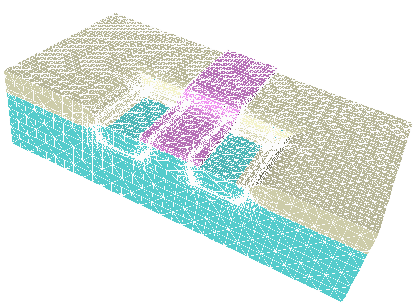
A first prototype of geometry/field server in 2D conformed to minimal SWR specification is the FOREST tool developed by our group. Later on the level-set boundary movement for geometry, CAMINO (quad/oct tree) and EUCLID (unstructured triangles and tetrahedra) have been developed according to minimal SWR. Examples for gridded device structure are shown in Figure 4. Simulation tools such as ALAMODE and SPEEDIE have been connected to the gridders according to the minimal SWR specification and an inter-operable suite of TCAD tools has been shown in the SUPREM OO7 framework, consistent with our vision in Figure 1.
Test cases of 3D multi-region MOS structures gridded by CAMINO have been validated with the Fermi diffusion model implemented in ALAMODE. The Oct-tree based tetrahedral mesh contains anisotropic refinement capabilities and can take general boundary-representation geometry. The generalized oct-tree mesh generation algorithm enables mesh refinement and de-refinement in different directions at various regions. A vector level control function is computed and indicates the directions for which the refinement will be performed. In a contour based refinement scheme, the level control function indicates the directions as the gradient, while in an error estimator based scheme, it indicates the direction where the error will be maximally reduced. Every octant can be refined in either one, two or three dimensions. After the tree is generated, detailed tetrahedralization algorithms are implemented to match the complex geometry and ensure mesh conformity. Then after each simulation step, the vector level control function is re-calculated according to the new gradient or error, and the mesh is adapted to reflect the changing areas of simulation significance. With the tree structure, interpolation error is also greatly reduced since the meshes before and after the adaptation share many common nodes. Grid quality required by the maximum principle is also derived.
The use of 1D parameters or 2D profiles in creating 3D structures through geometry modelers such as VIP-3D has potential limitations to accurately include important 3D effects. For example, 3D LOCOS structures generated in this way do not show the effects of enhanced oxidant diffusion at mask corners. A new capability to integrate simulated 3D surfaces has been used in VIP-3D to generate more accurate wafer structures. We have chosen a quasi-3D LOCOS modeling algorithm, which uses a combination of parameterized 2D analytic bird's beak shape equations and a fully 3D oxidant diffusion simulation based on the boundary element method to model corner effects in local oxidation. 2D and 3D simulations are combined in order to reduce computational cost. This heterogeneous approach reduces overall complexity which mirrors the goal of VIP as a means for rapid prototyping.
ALAMODE has been selected as the benchmark platform for the bulk diffusion models developed under the SRC/National Labs CRADA projects. A common 1D field interface is defined by Dr. Martin Giles of Intel to facilitate easy calibration process. Extension to 2D and 3D with various element technology is readily available in ALAMODE. Due to the dial-an-operator design and many finite-element numerical control in ALAMODE, new models and their numerical algorithms will be entirely encapsulated in the extension language level without touching the source code, and hence eliminate problematic comparisons of physical models implemented on most EWS platforms. Owing to its flexible and portable features for implementing advanced (PDE) models in a common (TCL) scripting language, easily shared between industrial groups and the national labs, the results of the SPRINT-CAD project have had a major impact on the SRC/DoE CRADA. This first-time demonstration is a breakthrough in changing the paradigm for how to develop and share advanced process models. ALAMODE has also been tested in many other industrial companies and universities participating in the SRC (SUPREM) process simulation project. A full user manual is also available in both postscript and HTML formats. A graphical user interface (GUI) is also developed, which operates under the Stanford Desktop environment.
Gridding has perpetually been a difficult part for practical TCAD applications. Requirements on gridding for accurate 2D/3D simulation have been discussed with Intel, primarily on the MOS transistors and isolation structures. Gridding tools developed at Stanford such as CAMINO and EUCLID, together with the SWR API interface, have been considered for resolving the complex geometry features. The development of the geometry/field server concept and the functionalities provided by the level-set boundary movement and quad/oct tree adaptivity has been realized in a popular release of SPEEDIE, which is integratable to all other SUPREM OO7 simulation modules.
[2] S. Osher and J.A. Sethian, "Fronts Propagating with Curvature-dependent Speed: Algorithms based on Hamilton-Jacobi formulations," J. Comp. Phys., vol. 79, pp. 12-49, 1988.
[3] M. Lobo,et. al., "The discrete maximum principle in finite-element thermal radiation analysis," Numerical Heat Transfer, Part B (fundamentals), vol. 24, no. 2, pp. 209-227, Sept. 1993.
[4] Z.H. Sahul, K.C. Wang,Z-K. Hsiau, E.W. McKenna and R.W. Dutton, "Heterogeneous Process Simulation Tool Integration," IEEE Trans. Semi. Manu., vol. 9, no. 1, pp. 35-48, Feb. 1996.
[5] W. B. Richardson and B. J. Mulvaney, "Plateau and Kink in P Profiles Diffused into Si: A Result of Strong Bimolecular Recombination," Appl. Phys. Lett., vol. 53, no. 20, pp. 1917-1919, 1988.
[6] T. Kunikiyo, "Calculation Results of Hane Model by Alamode," private communication, 1996.
[7] J.J. Hsieh, "Influence of Surface-activated Reaction Kinetics on Low-pressure Chemical Vapor Deposition Conformality Over Micro Features," J. Vac. Sci. Tech. A., vol. 11(1), pp. 78-86, 1993.
2. S. Beebe, F. Rotella, Z. Sahul, D. Yergeau, G. McKenna, L. So, Z. Yu, K.C. Wu, E. C. Kan, J. McVittie and R. W. Dutton, ``Next generation Stanford TCAD -- PISCES 2ET and SUPREM OO7, '' IEDM Tech. Digest, 1994, p. 213.
3. D. W. Yergeau, E. C. Kan, M. Gander and R. W. Dutton, "ALAMODE: a layered model development environment, '' Simulation of Semiconductor Devices and Processes, eds. H. Ryssel and P. Pichler, 1995, p. 66.
4. R. W. Dutton and E. C. Kan, "Hierarchical process simulation for nano-electronics," invited paper, International Workshop on Computational Electronics, Tempe, AZ, Nov. 1995.
5. Z. Hsiau, E. C. Kan, J. P. McVittie and R. W. Dutton, "Physical etching/deposition simulation with collision-free boundary movement, '' IEDM Tech. Digest, 1995, p. 101.
6. Z. Hsiau, E. C. Kan, D. S. Bang, J. P. McVittie and R. W. Dutton, "Modeling and characterization of 3D effects in physical etching and deposition simulation," SISPAD'96 (International Conference on Simulation of Semiconductor Processes and Devices), Tokyo, Sept. 1996.
7. K. Wang, H. Park, Z. Yu, E. C. Kan and R. W. Dutton, "3D Solid Modeling of IC Structures Using Simulated Surface Topography," SISPAD'96, Tokyo, Sept. 1996.
8. T. Chen, J. Johnson, and R. W. Dutton, "A Vector Level Control Function for Generalized Octree Mesh Generation," SISPAD '96, Tokyo, Sept. 1996.
9. N. Golias and R. W. Dutton, "Advanced Geometric Techniques in 3D Process Simulation," SISPAD '96, Tokyo, Sept. 1996.
10. Z. Hsiau, E. C. Kan, J. P. McVittie and R. W. Dutton, "2D/3D Etching and Deposition Simulation Tools Implemented with a General TCAD Geometry Server," Techcon'96, Pheonix, AZ, Sept. 1996.
11. Z. Hsiau, E. C. Kan, J. P. McVittie and R. W. Dutton, "Robust, stable and accurate boundary movement for physical etching and deposition simulation," to be published in IEEE Trans. Electron Devices.
12. S. Onga, T. K. Okada, H. Takada, T. Koyanagi, E. C. Kan and R. W. Dutton, "Hierarchical simulation for ULSI process design: from atomistic to conventional process CAD, '' invited talk, Intl. Workshop on Comp. Elec.(IWCE), Notre Dame, IN, May 1997.
13. E. C. Kan, L. Wang, D. W. Yergeau, P. Losleben and R. W. Dutton, "SUPREM OO7: User Interface and Geometry/field Server," software showcase in IWCE, Notre Dame, IN, May 1997.
14. E. C. Kan, Z. K. Hsiau, V. Rao and R. W. Dutton, "Gridding Techniques for the Level Set Method in Semiconductor Process and Device Simulation," to be presented in SISPAD'97, Boston, Sept. 1997.
15. V. S. Rao, T. J. R. Hughes, E. C. Kan and R. W. Dutton, "A New Numerical Formulation for Thermal Oxidation," to be presented in SISPAD'97, Boston, Sept. 1997.
Appendix B: Excerpt (Chapter 6) from Ph.D. dissertation by Ze-Kai Hsiau on "Boundary Movement in Semiconductor Etching and Deposition Simulation," 1997.
Appendix C: Excerpts from Ph.D. dissertation (not final format) by Vinay Rao on "On the Numerical Modeling of Thermal Oxidation of Silicon," 1997.
Appendix D: M. J. Gander and D. W. Yergeau, "The maximum principle in finite Elements," unpublished report.