
last updated Dec 19, 1999
![]()
![]()
![]()
![]()
![]()
![]()
![]()
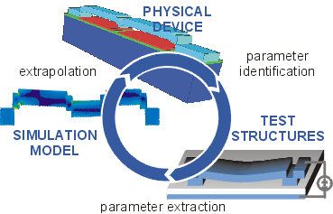
The goal is to characterize a fabrication process and calibrate a simulator to help a designer optimize device designs. We have a device that we want to build. First, we need to identify some basic parameters that determine the performance of this device such as geometry or shape, and material properties. Then we design test structures that isolate these parameters allowing accurate parameter extraction. All this information is stored in a detailed simulation model which can then be used to design or extrapolate the performance of the actual device.
Straightforward enough but many engineers stop at various points along the wheel. Either they perform parameter extraction without going on to the design and extrapolation step, or perform simulations without using real extracted parameters, just hoping to get lucky. All the steps must flow consistently to be confident that we know what's really going on.
![]()
Test
Structures
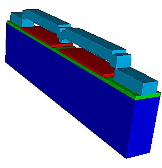
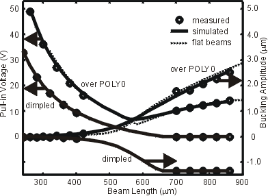
Fixed-fixed
beams of various lengths are fabricated. Discontinuities - steps
over POLY0, and dimples - are characterized explicitly. Buckling
amplitudes are measured using an optical profilometer. Pull-in
voltages are then measured using a CV meter. The boundary conditions
are designed to be essentially 2D to match simulations better.
Characterization
of flat beams
(table
of data)
Characterization
of beams with discontinuities
(table
of data)
Layout (GDS
II or CIF)
(click
on picture for larger image)
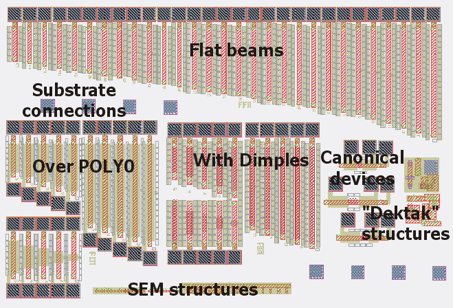
Composite CAD Process Definition Specification
![]()
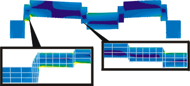
Simulation
This
two-dimensional computer simulation model capturing the various
discontinuities forms a scalable simulation-based repository of
process information. Geometry and material properties than can be
passed on unambiguously to design engineers. This avoids the use of
fudge factors which are rather specific and often cryptic. An
electrostatic field subroutine that includes the effects of fringing
and finite plate thickness is incorporated into Abaqus to convert it
from a mechanical solver into an efficient coupled electromechanical
solver. Given the current state of computers and software, this is
the best tradeoff between accuracy and speed for characterization purposes.
Simulation parameters
|
Measured Thicknesses (microns) |
|
|
POLY0 (with gold) |
0.52 |
|
POLY0 (without gold) |
0.53 |
|
POLY1 |
1.97 |
|
Dimple depth |
0.67 |
|
Sacrificial PSG |
1.79 |
|
Nitride (electrical) |
0.077 |
|
Stepup sidewall |
2.10 |
|
Extracted Properties |
|
|
Initial biaxial stress |
6.3 MPa |
|
Young's modulus |
140 GPa |
Simulated beam
(Abaqus input
decks)
![]()
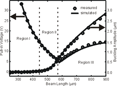
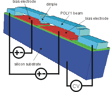
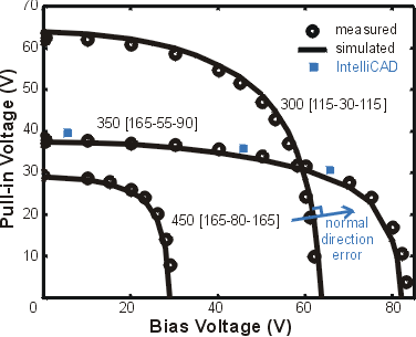
Extrapolation
The
well-calibrated simulation model is then used to predict the
behavior of more complex dual-electrode structures. The voltage at
one electrode required to pull the beam center onto the nitride is
measured as a function of the bias voltage applied to the other
electrode. The extrapolation is excellent confirming the validity of
the extraction procedures and the viability of these measurements as
benchmarks for coupled electromechanical simulators.
![]()
Measured
and simulated pull-in voltages
(table
of data)
![]()