Set coefficients of vacancy kinetics.
SYNOPSIS
- vacancy
-
( silicon | oxide | poly | oxynitr | nitride | gaas | gas )
[ D.0 = n ] [ D.E = n ]
[ Kr.0 = n ] [ Kr.E = n ]
[ Cstar.0 = n ] [ Cstar.E = n ]
[ ktrap.0 = n ] [ ktrap.E = n ]
[ neu.0 = n ] [ neu.E = n ]
[ neg.0 = n ] [ neg.E = n ] [ dneg.0 = n ] [ dneg.E = n ]
[ tneg.0 = n ] [ tneg.E = n ]
[ pos.0 = n ] [ pos.E = n ] [ dpos.0 = n ] [ dpos.E = n ]
[ tpos.0 = n ] [ tpos.E = n ]
[ ( /silicon | /oxide | /poly | /oxynitr | /nitride | /gaas | /gas ) ]
[ time.inj ] [ growth.inj ] [ recomb ]
[ Ksurf.0 = n ] [ Ksurf.E = n ]
[ Krat.0 = n ] [ Krat.E = n ]
[ Kpow.0 = n ] [ Kpow.E = n ]
[ vmole = n ] [ theta.0 = n ] [ theta.E = n ]
[ Gpow.0 = n ] [ Gpow.E = n ]
[ A.0 = n ] [ A.E = n ] [ t0.0 = n ] [ t0.E = n ]
[ Tpow.0 = n ] [ Tpow.E = n ]
[ rec.str= ] [ inj.str= ]
DESCRIPTION
This statement allows the user to specify values for coefficients of the vacancy continuity equation. The statement allows coefficients to be specified for each of the materials. Of course, the meaning of a lattice vacancy in an amorphous region is a philosophical topic. SUPREM-IV has default values only for silicon and the interfaces with silicon and gallium arsenide and its interfaces. Polysilicon has not been characterized as extensively, and its parameters default to those for silicon.
The vacancies obey a complex continuity equation which can be written [1]:
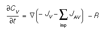
whereCV is the vacancy concentration, JV refers to the vacancy flux, JAV refers to the flux of impurity A diffusing with vacancies, and R is all sources of bulk recombination of vacancies. In the two.dim model (see method) the fluxes from the dopants, JAV, are ignored. Only in the full.cpl model are they computed and included in the vacancy equation. This model represents the diffusion of all vacancies, paired or unpaired, and can be derived from assuming thermal equilibrium between the species and that the simple pairing reactions are dominant [1].
The pair fluxes are the vacancy portions of the flux as described in each of the models for the impurities (see the various impurity statements). The vacancy flux can be written [1]:
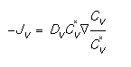
It is important to note that the equilibrium concentration, C*V, is a function of Fermi level [3]. This flux accounts correctly for the effect of an electric field on the charged portion of the defect concentration. The bulk recombination is simple interaction between interstitials and vacancies. This can be expressed:
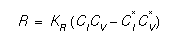
where KR is the bulk recombination coefficient, and CI and C*I are the interstitial and interstitial equilibrium concentration, respectively.
The defects obey a flux balance boundary condition, as described by Hu [4]:
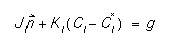
where  is the surface normal, KV is the surface recombination constant, and g is the generation, if any, at the surface. This expression has been used with success on several different surface types.
- silicon, oxide, poly, oxynitr, nitride, gaas, gas
- These parameters allow the specification of the material for which the parameters apply.
- D.0, D.E
- These floating point parameters are used to specify the diffusion coefficient of the vacancies. The units are in cm2/sec. The default values are 6.34E3 cm2/sec and 3.29 eV [5] for silicon, and 1.0E-12 cm2/sec and 0.0 eV for GaAs.
- Kr.0, Kr.E
- These floating point parameters allow the specification of the bulk recombination rate in cm3/sec. The default is 1.4 cm3/sec and 3.99 eV [6] for silicon, and 1.0E-18 cm3/sec and 0.0 eV for GaAs.
- Cstar.0, Cstar.E
- These parameters allow the specification of the total equilibrium concentration of vacancies in intrinsically doped conditions. The default values are 4.77E18 cm-3 and 0.713 eV [5] for silicon, and 4.77E14 cm-3 and 0.0 eV for GaAs.
- neu.0, neu.E, neg.0, neg.E, dneg.0, dneg.E, tneg.0, tneg.E, pos.0, pos.E, dpos.0, dpos.E, tpos.0, tpos.E
- These values allow the user to specify the relative concentration of interstitials in the various charge states (neutral, negative, double negative, triple negative, positive, double positive, and triple positive) under intrinsic doping conditions. For example, in intrinsic conditions, the concentration of doubly negative interstitials is given by:
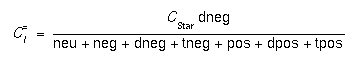
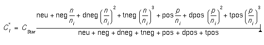
where CStar is the total equilibrium concentration in intrinsic doping conditions. In extrinsic conditions, the total equilibrium concentration is given by [3]:
-
- There is very little data for the vacancy charge states; it is matter of ongoing research. The default values for silicon are chosen based on an analysis and measurements of Watkins [7].
See Table 4 in the section "Adding SUPREM 3.5's GaAs Models and Parameters to SUPREM-IV" for GaAs values.
- /silicon, /oxide, /poly, /oxynitr, /nitride, /gas, /gaas
- These parameters allow the specification of the interface for which the boundary condition parameters apply. For example, parameters about the oxide silicon effect on vacancies should be specified by listing silicon /oxide. Only one of these can be specified at a time.
- time.inj, growth.inj, recomb
- These parameters specify the type of reactions occurring at the specified interface. The time.inj parameter means that a time dependent injection model should be chosen. The growth.inj parameter ties the injection to the interface growth velocity. The recomb parameter indicates a finite surface recombination velocity.
- Ksurf.0, Ksurf.E, Krat.0, Krat.E, Kpow.0, Kpow.E
- These parameters allow the specification of the surface recombination velocity. The formula used in computing the actual recombination velocity is:
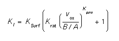
where vox is the interface velocity, and B/A is the Deal Grove oxide growth coefficient (see oxide). The full model applies only to oxide, since it is the only interface that can grow in SUPREM-IV. This formulation allows an inert interface to have different values than a growing interface. For inert interfaces, (gas, oxynitride, nitride, poly) KSurf is the only important parameter.
- vmole, theta.0, theta.E, Gpow.0, Gpow.E
- These parameters allow the specification of generation that is dependent on the growth rate of the interface. The formula is:
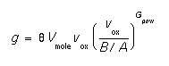
Theta,  , is the fraction of silicon atoms consumed during growth that are reinjected as vacancies. Vmole is the lattice density of the consumed material. Once again, this model only makes sense for oxide since it is currently the only material which can have a growth velocity.
- A.0, A.E, t0.0, t0.E, Tpow.0, Tpow.E
- These parameters allow an injection model with a fairly flexible time dependency. The equation for the injection is:
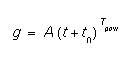
where t is the time in the diffusion in seconds. This can be used to represent the injection of vacancies from an nitride layer.
- rec.str, inj.str
- These two string parameters are useful for experimenting with new models for injection or recombination at interfaces. Three macros are defined for use, t the time in seconds and x and y the coordinates. If these are specified, they are used in place of any other model. For example,
vacan silicon /oxide inj.str = (10.0e4 * exp( t / 10.0 ))
describes an injection at the silicon oxide interface that exponentially decays in time.
EXAMPLES
- vacan silicon Di.0=5.0e-7 D.E=0.0 Cstar.0=1.0e13 Cstar.E=0.0
- This statement specifies the silicon diffusion and equilibrium values for vacancies.
- vacan sil /oxi growth vmole=5.0e22 theta.0=0.01 theta.E=0.0
- This parameter specifies the oxide - silicon interface injection is to be computed using the oxide growth velocity and with 1% of consumed silicon injected as vacancies.
- vacan silicon /nitride Ksurf.0=3.5e-3 Ksurf.E=0.0 Krat.0=0.0
- This specifies that the surface recombination velocity at the nitride silicon interface is 3.5E-3 cm/sec.
- inter sil neu.0=1.0 neg.0=1.0 pos.0=0.0 dneg.0=0.0 dpos.0=0.0
inter sil neu.E=0.0 neg.E=0.0 pos.E=0.0 dneg.E=0.0 dpos.0=0.0
- This specifies that there are equal numbers of negative and neutral charged vacancies in intrinsic doping.
BUGS
There are no known bugs in this routine. However, the models used here are involved in ongoing research, and may by out of date at any time. Further, experimental verification is difficult. Many of the parameters have unknown dependencies on stress, temperature, starting silicon material, stacking fault density, etc. High concentration phosphorus diffusion is promising with these models, but the coefficients have not been extracted to allow good fits to experiment.
REFERENCES
- M. E. Law and J. R. Pfiester, "Low Temperature Annealing of Arsenic/Phosphorus Junctions," IEEE Trans. on Elec. Dev., 38(2), p. 278, 1991.
- P.B. Griffin and J.D. Plummer, "Process Physics Determining 2-D Impurity Profiles in VLSI Devices," International Electron Devices Meeting, Los Angeles, p. 522, 1986.
- W. Shockley and J.T. Last, "Statistics of the Charge Distribution for a Localized Flaw in a Semiconductor," Phys. Rev., 107(2), p. 392, 1957.
- S.M. Hu, "On Interstitial and Vacancy Concentrations in Presence of Injection," J. Appl. Phys., 57, p. 1069, 1985.
- T.Y. Tan and U. Gosele, "Point Defects, Diffusion Processes, and Swirl Defect Formation in Silicon," J. Appl. Phys., 37(1), p. 1, 1985.
- M. E. Law, "Parameters for Point Defect Diffusion and Recombination," IEEE Trans. on CAD, Accepted for Publication, Sept., 1991.
- G.D. Watkins, "EPR Studies of the Lattice Vacancy and Low Temperature Damage Processes in Silicon," Lattice Defects in Semiconductors 1974, Huntley ed., 1975, Inst. Phys. Conf. Ser. 23, London.
- G.A. Baraff and M. Schluter, "Electronic Structure, Total Energies, and Abundances of the Elementary Point Defects in GaAs," Phys. Rev. Lett., 55, 1327 (1985).
SEE ALSO
The antimony,
arsenic,
beryllium,
boron,
carbon,
generic,
germanium,
interstitial,
magnesium,
phosphorus,
selenium,
isilicon,
tin,
and zinc statements