 ,
,
,
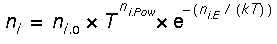
the values from the Blakemore expression were fit to this kind of equation for the temperature range of 500C to 1000C. From this, we determined that Ni0 = 4.0E16, Ni pow = 1.5, and Nie = 0.905.
SUPREM-IV also includes a fifth moment, the lateral straggle, in order to model the implantation profile in two dimensions. This moment was not determined for SUPREM 3.5, but in order to put some first-order numbers in for GaAs dopants, an algorithm based on TRIM results was developed. Even though TRIM does not predict the absolute values very well for GaAs, it does adequately predict trends and relationships. From tables of Pearson IV moments produced by TRIM for the dopants in GaAs, it is seen that ratio of the lateral straggle to normal straggle is fairly constant with implant energy for each ion, and that this ratio scales with the log of the ion mass. Assuming that this ratio is valid (as opposed to the actual values of the moments), we calculated this ratio for each ion and applied it to the experimentally determined normal straggles. From this, we determined that for each energy and dopant, the ratio of the lateral straggle (the fifth Pearson IV moment) to the normal straggle (the second Pearson IV moment) equals 1.83 - 0.525 log(ion mass). The lateral straggles for each dopant and energy were thus calculated and added to SUPREM-IV for the eight dopants in GaAs.
SUPREM 3.5 includes implant profile dependencies on dose and cap type and thickness. In general, we had experimentally determined that the tails decreased: (1) as the implant dose increased and (2) when the implants were done through oxide or nitride caps (in addition to changing the projected range). Both these phenomena are presumably due to decreasing the ion channeling, either by randomizing the ion trajectory or by decreasing the channels. This is modeled in SUPREM 3.5 by adding an algorithm which modifies the second Pearson-IV moment as a function of dose or cap. SUPREM 3.5 is able to do this because the complete processing history is part of the structure information file. There is no capability for this in SUPREM-IV, and will have to be added later.
SUPREM-IV.GS now allows one to specify the implant angle. Experimental determination of implant parameters for GaAs showed that the channeling was minimized for implant angles of greater than or equal to 10 degrees to the normal, and the default parameters correspond to that condition. For now, specifying and angle of less than 10 degrees will not increase the channeling in the simulations (that will be added later), but "shadowing" is now simulated for non-zero degree implants.
 (EQ 1)
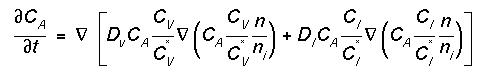
where C is concentration, D is diffusivity, V is vacancy, I is interstitial, and the "star" denotes equilibrium values. For p-type dopants, the electron concentration, n, is replaced by the hole concentration, p. It is assumed that the diffusion occurs via interstitials or vacancies, or a combination of both. The full expressions for Dv and Di, which are dependent on the fermi-level and on the fraction of interstitial-assisted diffusion (Fi ), as compared to that which diffuses via vacancies, are given in Table 1.
TABLE 1 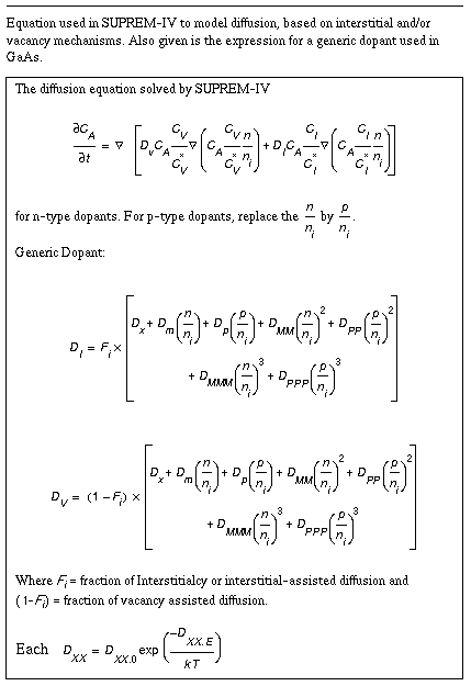
We have previously determined that the four n-type dopants in GaAs diffuse via a Ga vacancy mechanism (Fi = 0) and that the p-type dopants diffuse via a Ga interstitial mechanism (Fi = 1) [1-4]. We have also shown that the kick-out (or substitutional-interstitial diffusion mechanism), traditionally used to model p-type diffusion in GaAs, results in virtually identical governing diffusion equations as used for interstitial diffusers in SUPREM-IV for Si [4]. We have demonstrated that SUPREM-IV's equation can be used to successfully model the anomalous diffusion behavior of Mg in GaAs when excess defects produced by implant damage are included. For these reasons, it has been a relatively simple task to incorporate SUPREM 3.5's simple non-defect models and parameters into the SUPREM-IV framework. Basically, the expressions in SUPREM 3.5 were made to be the Di and Dv terms for p-type dopants and n-type dopants, respectively [See the 1990 and 1992 Stanford Technical Reports, "Process Simulators for Silicon VLSI and High Speed GaAs Devices," by Plummer, et al. for more discussion on these values]. Two simple modifications to SUPREM 3.5's expressions were made. One was to include a ni term in the expressions for the p-type dopants to fit the SUPREM-IV framework. In SUPREM 3.5, the diffusivity expressions were derived based on the kick-out methodology and were not normalized to the intrinsic carrier concentration. This modification involved changing the pre-exponential term and the exponential term (since Ni is a function of temperature) of the diffusivities. The other modification was due to the fact that the original n-type diffusivities were derived without an electric field effect. Since an electric field effect is built into SUPREM-IV's diffusion equation, the numbers had to be re-derived, since the effect can increase the total diffusion by up to a factor of two. All eight dopants were tested in SUPREM-IV (without any excess interstitials or vacancies) to ensure that their diffusion behavior for inert conditions is the same as SUPREM 3.5 predicts.
SUPREM 3.5 has two sets of diffusivities for Mg in GaAs, one for temperatures below 825C and one for temperatures above 825C. For now we use only the higher temperature values. Also, the diffusivity for grown-in Zn has been modified due to recent re-analysis of the literature data.
The equations and parameters for the eight dopants in regards to diffusion in GaAs are shown in Table 2 for the n-type dopants and in Table 3 for the p-type dopants.
TABLE 2 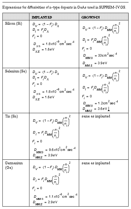
TABLE 3 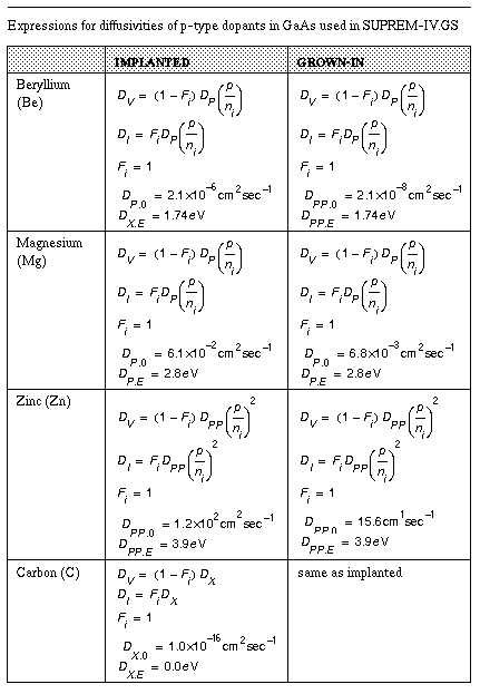
SUPREM 3.5 had two sets of diffusivities for dopants in GaAs: one for dopants that were implanted, and one for dopants that were incorporated during growth, or "grown-in." For p-type dopants, the implanted values are generally higher than the grown-in; for n-types the implanted values are generally lower than the grown-in. These differences are believed to be due to different point defect conditions caused by the introduction of the dopants and the subsequent diffusion. For this first version of SUPREM-IV.GS, we have used the SUPREM 3.5 convention of using different values of D for the two cases (in the future, physically correct models which take into account the different point defect conditions will be used). SUPREM-IV.GS keeps track if a given dopant has been implanted or not, and uses the appropriate value. (It assumes that if the dopant is not implanted, it is grown-in. Gas source diffusions would therefore use the grown-in values). If you want to use the implanted value for cases where the dopant is not implanted in the input file (e.g. when a solid-source diffusion is done, or when a SIMS file is used as the initial dopant profile), then one should do a very low dose implant (i.e. below the background level) of that dopant so the program thinks that all of it has been implanted.
The SUPREM 3.5 default numbers for dopant diffusivity in cap material (silicon oxide or nitride) used in GaAs technology have been added to SUPREM-IV, as have the segregation and transport values across interfac es. Rather arbitrary default numbers for interstitial and vacancy diffusivity, segregation, and transport parameters have also been added. These will be updated when more reliable numbers are determined.
We have also added a generic dopant to SUPREM-IV.GS, whose diffusivity expression is shown in Table 1. This includes many n and p terms in the expression and can be used to test other dopants and diffusivities for subsequent model development. (The default type of the generic dopant is an acceptor.)
Since some dopants in GaAs are amphoteric and can be either donors or acceptors under certain conditions, we have added the capability of changing the type of the impurity from its default to either donor or acceptor. This is an impurity specification option.
We have decided to model dopant activation for GaAs in SUPREM-IV using the second method. This is believed to be the more physically correct model for the phenomena and will result in the compensation ratio, or fraction inactive, to be based on the total doping, which is what is actually observed, and not on each dopant individually, which is what is done in SUPREM 3.5.
Until a defect-based compensation model is incorporated into SUPREM-IV, a semi-empirical model will be used. The original algorithm in SUPREM 3.5, in addition to having the shortcomings mentioned above, was based on limited data in the literature and resulted in errors at high concentrations and temperatures. An expression for the compensation effect has been determined by fitting recent modeling results of Vanasupa [6] with an analytical equation, which is a function of net doping concentration, , and temperature. (Vanasupa's numbers are based upon both experimental data and a specific compensation mechanism, compensation by amphoteric pairs in her case, but the numbers would apply to any compensation mechanism.) The equation is:
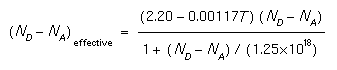 (EQ 2)
where T is in degrees Kelvin. The compensation factor will be applied to the net doping concentration calculation to get an effective net doping concentration.
The expression for compensation is based on the equilibrium activation numbers of Vanasupa [6]. She also determined that there is a time dependent, kinetic part to the activation process, important for short time activation anneals. This will also have to be included in future models for dopant activation in GaAs.
The solubility values for dopants in GaAs are not well known. Until good numbers are obtained, default values of 11019 cm3 will be used for all dopants.
SUPREM 3.5 does not consider point defects in its implantation, diffusion, or activation models. As discussed above, one of the prime motives for incorporating GaAs into SUPREM-IV is to make use of SUPREM-IV's point defect capabilities, especially in regards to the effect of point defects on dopant diffusion and activation. For the initial version of SUPREM-IV for GaAs, we want to include some default numbers for the defect parameters so we can start our development of future point-defect based models for diffusion and activation.
SUPREM-IV only considers one type of interstitial and one type of vacancy. In GaAs there are two types of each: Ga and As. Eventually we will have to add both types to SUPREM-IV, but for now we will only assume one type. (We have shown that for modeling diffusion of both n-type and p-type dopants in GaAs, it is not a bad assumption to consider only the Ga sublattice (see reference [4] for example), so this limitation may not hinder us too much.)
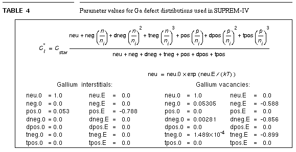
The total number of defects and the distribution of each charge type is calculated by SUPREM-IV as a function of temperature and fermi-level. Using the energy levels of the variously charged vacancies and interstitials calculated by Baraff and Schluter [7] and by Jansen et al. [8], the relative probability of each charge state was calculated using the Shockley-Last equations [9]. These numbers are given in Table 4. Since triply charged interstitials and vacancies are important in GaAs, and SUPREM-IV previously only included neutral through doubly charged defects, new parameters had to be added.
Rather arbitrary default numbers for defect recombination (both surface recombination and bulk I/V recombination) have been put in for Ga interstitials and vacancies.