
last updated June 3, 1999
![]()
![]()
![]()
![]()
![]()
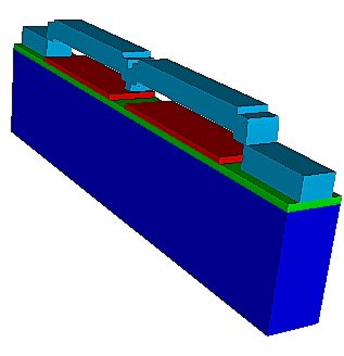
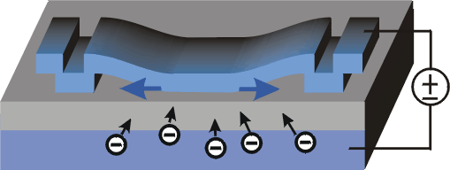
When the polysilicon beam contacts the underlying nitride layer, the system behaves like a variable capacitor that is very sensitive to contact conditions. By measuring the changes in capacitance as a function of applied voltage and time, effective surface compressibility and dielectric charging can be measured.
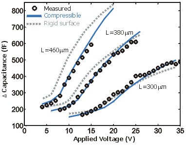
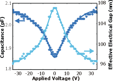
Measured and simulated CV curves
Dielectric
Charging
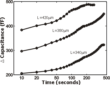
The
capacitance of the system continues to increase with time as the
voltage is held steady. This is due to charge buildup in the nitride
which increases the attractive force on the polysilicon beam. The
rate of charging corresponds to charge injection through direct tunneling.
![]()
Surface
Effects
The measured CV
curves could not be matched by simulations assuming ideal contact
conditions. A compressible surface model allows the effective gap
between the polysilicon beam and substrate to decrease with applied
voltage (and hence applied surface pressure). This compression effect
could be due to asperities or surface residue distributed over the
contact surfaces. This general behavior is verified by the CV
measurement of a flat plate where no zipping occurs yet the
capacitance still increases with voltage.
CV curve of flat plate (no zipping)
![]()