
Current Project: I/O Scaling for Improved Performance and Charged Device Model (CDM) Protection
Our current project focuses on design methodology development aimed to address reliability concerns including transistor level breakdown mechanism and electrostatic discharge (ESD) protection during the design phase. Spice-compatible models of transistor degradation are developed and enhanced for sub-45nm technologies, including variability issues, using TCAD. At multi-GHz frequencies, the limited capacitive budget for ESD protection requires optimization as part of design; bus and protection device resistance also limits the protection of I/O devices. To guarantee protection levels for high current CDM stress, design methods are developed to prevent excessive voltage build-up across these devices. Trade-offs between protection level and performance impact are evaluated and optimized. Results of modeling and optimization will be validated.
Our current ESD research has been sponsored by Center for Integrated Systems (CIS) and Advanced Micro Devices (AMD) FMA fellowship, as well as Semiconductor Research Corporation (SRC) Global Research Collaboration (GRC) fellowship. Industry mentors are Dr. Stephen Beebe from Advanced Micro Devices and Dr. Timothy Maloney from Intel Corporation.
Previous project sponsors include LSI Corporation and Texas Instruments Inc.
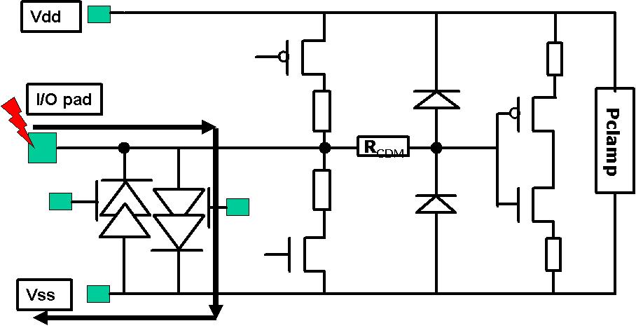
Figure 1: Local clamping ESD protection scheme for aggressively scaled high-speed I/O circuit
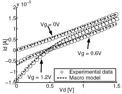
Figure 2: Macro-Model for ESD breakdown (including ELF application) and experimental data for 130nm device (post breakdown). Scaling parameters for the model allow it be used for automated screening of robustness in cell libraries and at the chip level [T.W. Chen et al, IRPSX, pp. 78-85, 2007]
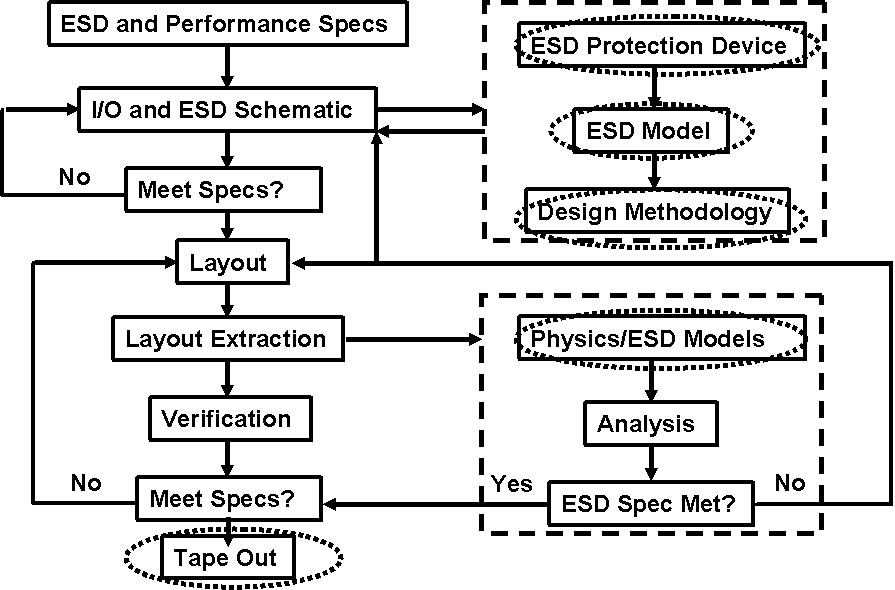
Figure 3: Flow chart depicting design for reliability methodology [S. Cao and R. Dutton, 2008 SRC GRC Annual Review]
List of Ph.D. graduates, research associates and current students working on ESD research:
Dr. Kaustav Banerjee (Previously research associate)
The work of our ESD team has been repoted by ESD Association magazine (page 7)
Previous Projects
Previous ESD projects address modeling and simulation of circuit design issues related to ESD with emphasis on high-performance interface circuits for RF and A-to-D applications. Ongoing scaling of MOS technology has imposed more stringent requirements on ESD protection devices. At the same time, performance of the circuits can be seriously compromised by the protection devices. Recent accomplishments of this project include: considerations of LNA design and matching networks (joint with Infineon) and dynamic range and linearity considerations of ADCs (joint with Texas Instruments).
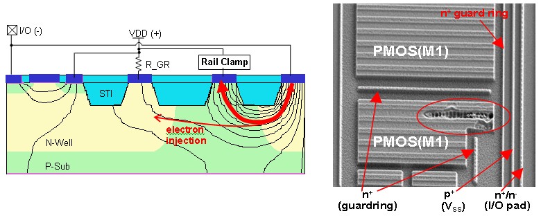
These results show 2D device simulations of current flow in an ESD protection structure using a diode rail clamp. The larger arrow in the left figure indicates intended flow path of current to the diode; the longer arrow indicates bipolar transistor current flow to the n-well, which causes non-uniform triggering of ESD protection devices. These simulations have been correlated with test structure results (the circle in the figure below indicates the site damaged by this non-uniform triggering), courtesy Dr. Duvvurry, Texas Instruments (IRPS 2004)
For details about the past ESD research projects, please follow the link of the graduates' names for the research abstract and Ph.D. thesis.
Last updated October 28, 2008.
All rights reserved. ©2008 Board of Trustees of the Stanford University