#some set stuff
set echo

#the x dimension definition
line x loc = -2.0 tag = left
line x loc = 0.0 spacing=0.05
line x loc = 5.0 tag = right

#the vertical definition
line y loc = 0     spacing = 0.02 tag = top
line y loc = 1.5   spacing = 0.05
line y loc = 400.0                tag=bottom

#the silicon wafer
region silicon xlo = left xhi = right ylo = top yhi =
bottom

#set up the exposed surfaces
bound exposed  xlo = left xhi = right ylo = top  yhi =
top

#calculate the mesh
init boron conc=1.0e14

#the pad oxide
deposit oxide thick=0.02

#deposit the nitride mask
deposit nitride thick=0.05
etch nitride right p1.x=0.0 p2.x=0.0

#the boron implant
implant boron dose=3e14 energy=40 pearson

#the diffusion card
method two.d
diffuse time=30 temp=1100 dry

#save the data
structure out=oed.str
This example is very similar to Example 2. It starts by setting command line echoing and by instructing SUPREM-IV.GS to be relatively quiet about the progress of computation. The x line specification is different for the two dimensional device. For this example, an x line is placed at -2 microns and another at 5 microns for the left and right of the device. The area of most interest is the middle area near where the mask edge will be placed. Consequently, a tighter spacing is specified at the mask edge.
The next series of lines define the y lines, region, boundary, and initialize the wafer. A starting oxide is deposited and the boron implant is performed. These steps are all similar to Example 2.
Following the boron implant, a mask is deposited and etched.
#deposit the nitride mask
deposit nitride thick=0.05
etch nitride right p1.x=0.0 p2.x=0.0
The mask material is specified to be 0.05 microns of nitride. This will mask the oxide growth. The nitride is etched off to the right of a vertical line at x equal to 0 microns. The oxide will grow on the right and inject interstitials there.
The diffuse command contains the directive to simulate the 30 minute, 1100C drive-in and anneal.
#the diffusion card
method two.d init=1.0e-3
diffuse time=30 temp=1100 dry
The ambient is dry oxygen. This diffusion step will produce output similar to Example 2.
The next step is to save the data for further examination.
#save the data
structure out=oed.str
This saves the data in the file oed.str. This file can be read in using the init command or the structure command.
The following commands are not in an input deck, instead type them in to the simulator using the interactive facilities to plot and check data. The first command will be to read in the stored structure file. Type:
init inf=oed.strThis will read in the file and initialize the data structures of the program.
The final lines will plot the final boron concentration, in two dimensions
#plot the final profile
select z=log10(bor)
plot.2d bound fill y.max=2.0
foreach v (15.0 to 19.0 step 0.5)
   contour val=v
end
The first statement picks the log base ten of the boron concentration to plot. The next statement instructs SUPREM-IV.GS to plot the two dimensional outline of the device. The bound parameter asks for the material boundaries to be plotted. The area plotted will extend only down to y equal to 2 microns. The contour statements are plotted as part of loop. The foreach command repeats 9 times and sets the variable v to the value specified in the loop. Figure 1 shows that the lateral extent of the OED is well over two microns. There is little lateral difference in the shape of the profile.
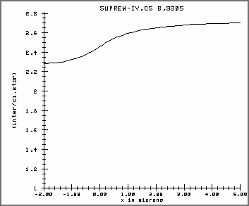
The interstitial concentration can also be plotted. This will verify that there is little lateral decay in the defect profile.
#plot the final profile
select z=(inter/ci.star)
plot.2d bound fill y.max=10.0
foreach v (1.25 to 3.0 step 0.25)
   contour val=v
end
Figure 2 shows the result. There is more shape to the defects than the boron. However, the profile is fairly flat across the top of the wafer.
The interstitial concentration can also be plotted in cross section and is shown in Figure 3.
plot.1d y.v=0.5This command will plot the interstitial concentration 0.5 microns below the surface.
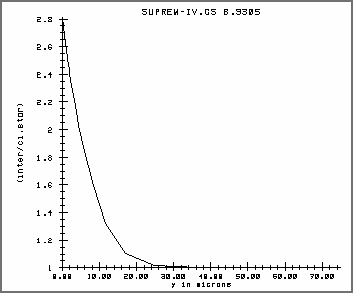
The value can also be plotted vertically, and is shown in Figure 4.
plot.1d x.v=5.0 x.ma=75.0This shows the penetration into the bulk of the interstitials. The penetration is limited by both the bulk recombination of the interstitials with vacancies and the trapping mechanism.