
In order to accelerate the design phase of new devices, simulation tools provide valuable insight into performance. For RF devices, Stanford and HP jointly developed an harmonic balance simulator for analyzing a device in the frequency domain[1]. However, the performance of this RF device is not restricted to intrinsic effects and can depend upon parasitics from interconnect and packaging as well as the matching networks and bias circuitry used to connect the device to the rest of the circuit. This paper addresses the RF simulation of the external circuit components in conjunction with the intrinsic device. The paper describes a simulation approach and presents an example of practical importance to industry.
The device under analysis is a LDMOS structure from Motorola (Figure 1)[2][3]. A laterally diffused graded channel enhances RF performance, prevents punch-through, and increases the device transconductance. A p+ sinker connects source and substrate together to eliminate extra bond wires and provide for a back side contact. An LDD decreases the electric field at the drain and a metal field plate reduces the electric fields at the edge of the gate.
Surrounding the device are a large number of circuit parasitics represented in block diagram form in Figure 2. Nearest the intrinsic device are the parasitics from interconnect resistances and capacitances. From the package, bond wires include inductances and outside the package, the bias circuitry and matching networks establish a connection to the rest of the circuit. The biasing circuitry is isolated from the input/output by inductors which block high frequencies while the matching networks are isolated with capacitors which block DC. Figures 3 and 4 show the experimental and simulated IV characteristics for the device.The device operates with up to 6V on the gate and 20V on the drain. The experimental Ids vs. Vds curves match the PISCES simulation using a local mobility model developed at Stanford[4]. Under high gate and drain biases, a high current generates heat, thus reducing the mobility; however, the device is rarely operated in this region. Figure 4 shows the good agreement for the Id vs. Vg curves in the linear region (Vd=0.1V) and saturations region (Vd=6.0V).
Stanford and HP jointly developed a PISCES extension that solves the semiconductor equations in the frequency domain thus enabling large signal sinusoidal simulations. However, circuit aspects from parasitics to matching networks play an important role in the actual utilization of the device.
To include the circuit components in the device simulation they are reduced to a set of boundary condition equations. Figure 5 shows a PISCES device surrounded by an arbitrary linear network. By assuming unknown voltages and currents at the electrodes of the device, the relationship among those voltages and currents are computed (refer to given Equation). For large signal AC analysis, the boundary conditions become complex and are calculated at each frequency. The Vapplied vector contains the source vector at DC and the fundamental frequencies. It is zero for the generated harmonics since the surrounding circuity is linear and hence, generates no new harmonics.
Circuit boundary conditions and harmonic balance simulation is integrated with PISCES as shown in Figure 6. PISCES calls the circuit boundary condition routines to generate the equations from a SPICE like netlist. It then calls the harmonic balance solver passing the boundary conditions and PISCES state variables. The harmonic balance solver uses the PISCES assembly routines to generate the Jacobian and RHS at each frequency for each iteration. Once the convergence criteria is met, the solution is passed back to PISCES which calls a circuit solver to get the complete solution.
This simulation algorithm is applied to the Motorola device to analyze its RF performance at 850MHz. The key design criteria are the power gain and the power added efficiency as shown in Figure 7. The gain rolls off at higher power levels (Pin > 15dbm) because the device is operating in the gm compression region and the output power is limited by the saturation current. The efficiency is low for a small Pin because the device drains more power in class A operation. Efficiency increases until just after the gain starts to decrease. At this point, Pin approaches Pout resulting in very little power added to the input signal. The simulation results in Figure 8 qualitatively follow the experimental results. Further tuning of the mobility models will improve the agreement.
Harmonic balance device simulation is a powerful tool for analyzing many types of RF problems. Coupling the device simulation with circuit parasitics and circuitry, extends the capabilities of the simulator to include not only the physical device but also an extrinsic components that ultimately affect the performance of the structure. This paper demonstrates the power of the tool by analyzing an LDMOS RF power transistor for gain and efficiency given parasitics, bias circuitry, and matching networks.
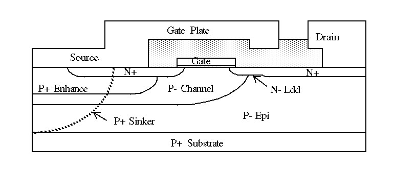 Figure 1: LDMOS device cross section.
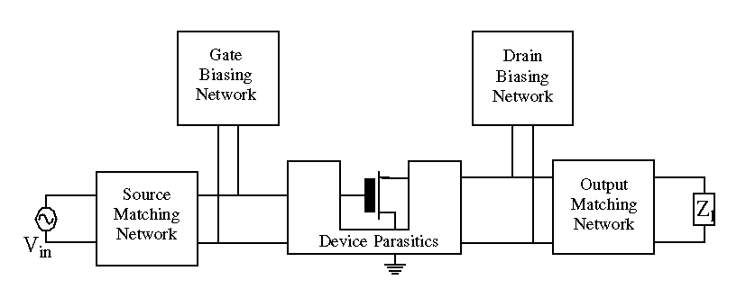 Figure 2: Block diagram of amplifier circuit including
biasing and matching network.
Figure 2: Block diagram of amplifier circuit including
biasing and matching network.
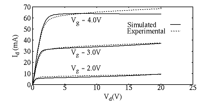 Figure 3: Simulated and experimental drain
characteristics.
Figure 3: Simulated and experimental drain
characteristics.
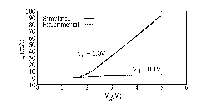 Figure 4: Simulated and experimental gate characteristics.
 Figure 5: PISCES device surrounded by an arbitrary
linear circuit.
Figure 5: PISCES device surrounded by an arbitrary
linear circuit.
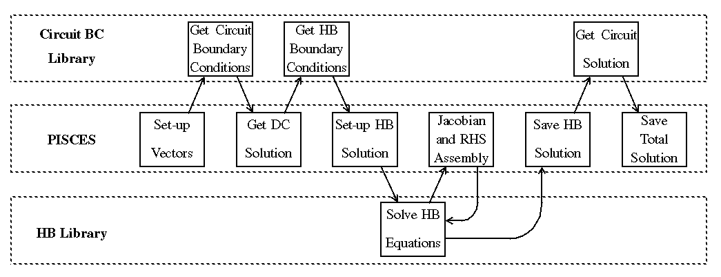 Figure 6: Integration of PISCES with linear
circuit BC's and harmonic balance.
Figure 6: Integration of PISCES with linear
circuit BC's and harmonic balance.
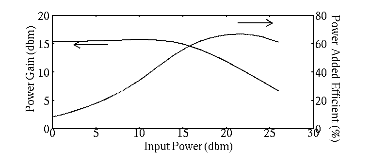 Figure 7: Experimental values for power gain
and power added efficiency.
Figure 7: Experimental values for power gain
and power added efficiency.
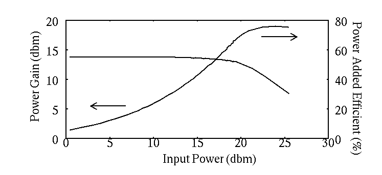 Figure 8: Simulated values for power gain and
power added efficiency.
Figure 8: Simulated values for power gain and
power added efficiency.