The two level Newton method for mixed circuit/device simulation incurs a significant computational cost. Mayaram had investigated that cost for a variety of algorithms including the two level Newton [3]. The most common of the alternate algorithms is the full Newton which Rollins had implemented previously [4].
In the full level Newton algorithm, the circuit matrix and device matrix are combined into a single matrix and all variables are solved simultaneously. As a result, the computational time is reduced, but there are trade-offs.
The two level Newton algorithm has the following advantages:
Likewise, there are a number of disadvantages to the two level Newton algorithm:
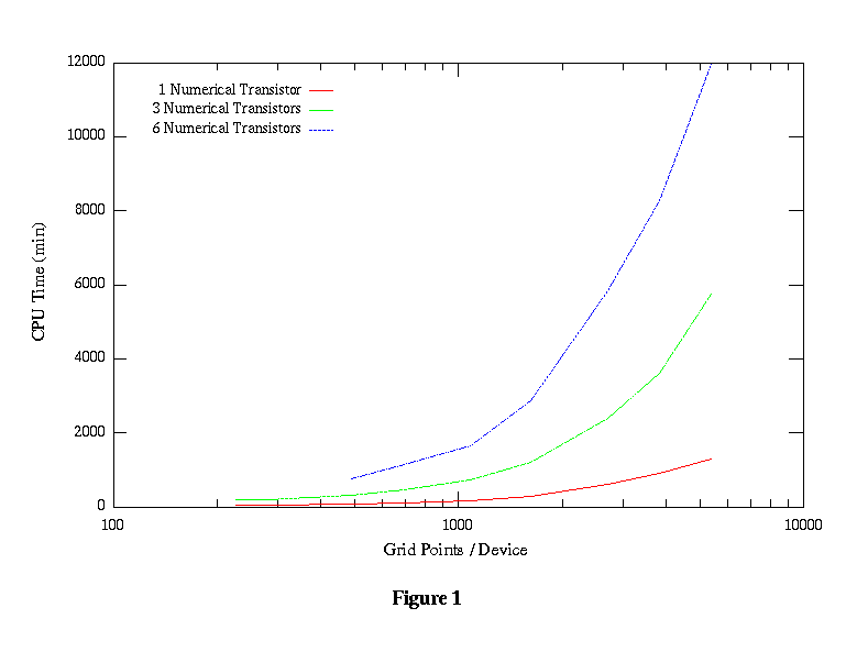
The SRAM example was used to analyze the computational time of mixed-mode simulation. The six transistor SRAM cell is simulated with a set of numerical devices containing a wide number of nodes for each device. In addition, three circuits are simulated. One circuit has only the pass transistor as a numerical device, another has half the cell (3 transistors) as numerical devices, and the third has all six transistors as numerical devices. The circuit was simulated to do a read/write cycle of a one and a zero so that each half of the cell is excersized in the same manner for when we don't have symentry. The non-numerical device transistors are modeled to approximate the numerical device characteristics.
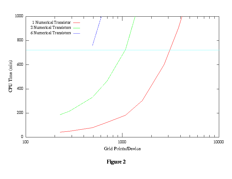
The simulations were executed on a single node of a SP1. The CPU time in minutes is shown in Figures 1 and 2. Figure 1 shows the total time for all the simulation runs. Figure 2 shows those that would take overnight or less with the light blue line representing the 12 hour mark with the fastest time being around 45 minutes. For the 6 numerical transistor circuit with minimal node devices, convergence became a problem and no data is available.