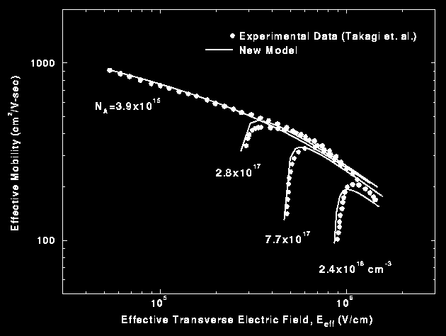
As MOSFETs scale to shorter channel lengths, channel doping levels increase in order to suppress undesirable short-channel effects such as punchthrough and drain-induced barrier lowering (DIBL). One direct consequence of increased doping is enhanced impurity scattering, the importance of which in scaled MOSFETs is established by demonstrating its impact on critical design parameters such as threshold voltage and off-state leakage current. An accurate model for impurity scattering has been developed that, for the first time, properly accounts for 2D confinement and quantum mechanical effects in the inversion layer. A systematic methodology for extracting Coulombic mobility from I-V data is also presented. Based on this scheme, it is shown that in regimes where three dimensional (3D) models grossly over-predict mobility, the new 2D model demonstrates its broad applicability by accurately reproducing experimental results over a wide range of channel dopings, substrate biases, and electron concentrations.
Traditionally, channel resistance has been the dominant factor limiting current transport in MOSFETs. However, in deep submicron MOSFETs with lightly-doped drain (LDD) structures, channel resistance has become comparable to the parasitic series resistance, a major component of which comes from the accumulation layer in the LDD region. A unified mobility model is presented that is applicable in both inversion and accumulation layers. A systematic methodology is presented for the calibration and validation of the new model with experimental data. Broad applicability of the new model is established with excellent agreement over a wide range of operating conditions (subthreshold, linear, and saturation) for gate lengths ranging from 20.0um down to 0.25um.
References:
[1] S.A. Mujtaba, R.W. Dutton, D.L. Scharfetter, "Semi-Empirical
Local NMOS Mobility Model for 2-D Device Simulation Incorporating
Screened Minority Impurity Scattering", to be presented at NUPAD V,
1994, Honolulu, Hawaii.
[2] S. A. Mujtaba, S. Takagi, R.W. Dutton, "Accurate modeling of Coulombic
scattering, and its impact on scaled MOSFETs," in Symp. VLSI Technol. Dig. Tech.
Papers, pp. 99-100, 1995.
[3] S. A. Mujtaba, M. R. Pinto, D. M. Boulin, C. S. Rafferty, R. W. Dutton, "An
accurate NMOS mobility model for 0.25mm MOSFETs," in Proc. 6th Intl. Conf.
Simul. Sem. Dev. Process. (SISDEP), pp. 424-427, 1995.
Aon Mujtaba (mujtaba@gloworm.Stanford.EDU)