option quiet
set echo

mode one.dim
line x loc=0.0 spacing=0.02 tag=top
line x loc=0.5 spacing=0.02
line x loc=20 spacing=0.25 tag=bottom

region gaas	xlo=top  xhi=bottom
boundary exposed xlo=top xhi=top
boundary backside xlo=bottom xhi=bottom

init beryllium conc=3e17
implant isilicon dose=5e13 energy=100 pearson

#material gaas p.type  act.a="(2.2 - 0.00117 * T)" act.b="1.00e21"
#material gaas n.type  act.a="(2.2 - 0.00117 * T)" act.b="4.25e18"

deposit nitride thick=.3
method fermi init=1e-5

diffuse time=.001 temp=750 argon
    select z=log10(isilicon)
    plot.1d x.mi=0 x.ma=2 y.mi=14 y.ma=20 line.type=1
    select z=log10(electrons)
    plot.1d x.mi=0 x.ma=2 y.mi=14 y.ma=20 cle=f axi=f line.type=2
    select z=log10(abs(doping))
    plot.1d x.mi=0 x.ma=2 y.mi=14 y.ma=20 cle=f axi=f line.type=3

quit
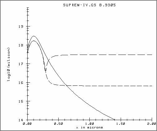
Silicon is implanted into GaAs with a beryllium doped background.
Figure 1
shows the 1D plot of this. The default n and p-type activation
models are used, commented out in the lines:
#material gaas p.type act.a="(2.2 - 0.00117 * T)"
act.b="1.00e21"
#material gaas n.type act.a="(2.2 - 0.00117 * T)"
act.b="4.25e18"
Plotted in Figure 1 are the silicon profile, the electron profile, and the net doping profile. The electron profile takes into account the less than 100 percent net n-type dopant activation under the silicon peak, as well as the reduced electron concentration in the bulk due to the beryllium background doping. The abs(doping) profile clearly shows the silicon/beryllium n/p junction.
Figure 2 shows the results when the n-type activation model parameters are changed. In this case, the following line is included:
material gaas n.type act.a="(2.2 - 0.00117 * T)" act.b="4.25e18"Note that the act.b parameter has been changed. This increases the net active n-type dopant concentration under the peak of the silicon implant profile.