DEVELOPMENT OF ANIMATED SIMULATION OF SEMICONDUCTOR ELECTRONIC DEVICES FOR CLASSROOM DEMONSTRATION
Constance J. Chang-Hasnain, James D. Plummer, Robert W. Dutton, and Zhiping Yu*
Electrical Engineering Department
Stanford University
Stanford, CA 94305-4085
Tel: (415) 723-0111; FAX (415) 725-2533
*on leave from Tsinghua University, Beijing, China
ABSTRACT
In this paper, we describe the development of animation videos based on
computer simulation of semiconductor electronic devices for classroom
demonstration of abstract concepts. The device physics taught in
junior-level required courses in electrical engineering are considered
and include: p-n diode, metal oxide semiconductor (MOS) capacitor, MOS
field effect transistor (FET), and bipolar junction transistor (BJT).
The concepts and methodology will be described, followed by several
examples.
INTRODUCTION
Since the first demonstration of diodes and transistors, semiconductor
electronic devices have continued to revolutionize our society through
an enormous number of inventions and applications built upon them.
Therefore, an introductory course on the basic concepts of
semiconductor electronic devices is generally considered essential for
all electrical engineering students, regardless of their final field of
specialization. Nevertheless, the fundamental physics of these devices
is of an abstract nature. Students with basic sophomore physics
training often have difficulty imagining electrons and holes in
semiconductors, let alone a p-n junction with electron and hole current
flows. Although they have usually, by this time, been introduced to
the fundamentals of quantum mechanics and of materials, a semiconductor
crystal with conduction and valence bands is very difficult to grasp
and visualize. It is based on this experience that the authors began
the development of animation video demonstrations of basic electronic
devices. The objective is to use animated simulation to provide a
visual-aid for understanding complicated concepts and the underlying
formula. In addition, the animations give students a clear grasp of
many physical parameters and their relative importance. Furthermore,
such animations will stimulate both interest for learning and deeper
understanding.
METHODOLOGY
The methodology of creating the animated
simulation movies is outlined in Figure 1. The devices of interest in
this project include p-n junction diode, p-i-n junction diode, MOS
capacitor, MOSFET and BJT. These devices were first simulated using
typical device parameters at various operating biases. The device
simulation program we used was TMA-MEDICI*, a commercial version of
PISCES (Dutton and Yu 1993), on a cluster of UNIXTM-based DEC
workstations. With each operating condition, a graph of data is
generated such as current vs. voltage (I-V) and capacitance vs. voltage
(C-V) characteristic curves, carrier and space charge distributions,
electron and hole current distributions, electric field distributions,
and energy band diagrams. For all the devices, the graphs can be made
into simple two-dimensional (2D) plots, 2D contour vector plots, or
three-dimensional (3D) plots. These graphs are captured and
transferred onto an Apple workstation using a graphics terminal
emulator (for example VersaTerm). A graphics application (for example
Canvas or MacDraw) is used to add artistic perception of electrons,
holes, and currents onto the band diagrams, and to touch up the
graphs. The animation is then done using MacroMind Director, an
animation package for Apple workstations. This program allows us to
combine various objects called cast members into a complete screen
frame. The cast members can be a PICT file, a combination of PICT
files, or a sound source. In our case, the frames can be calculated
plots generated by MEDICI for a specific device at various operation
conditions, e.g. biases. A motion picture of this device as one
changes the bias can thus be made by putting the frames in sequence.
In many cases, electrons and holes with appropriate motions are
included to exhibit current flows. Sound effects are also used to
enhance the demonstrations.
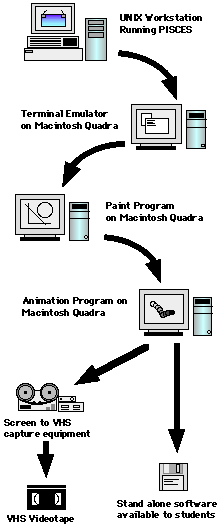
Fig. 1. Steps in creating animation of semiconductor electronic
devices. This method offers several advantages.
First, with the use
of MacroMind Director, movies in a variety of formats, i.e. multimedia,
can be generated. They can be exported to a video tape for classroom
demonstrations, to a Quicktime** movie to be played on Apple computers,
to presentation view graphs, or online movies. Secondly, there is a
great flexibility in devices to be simulated and even simulation
programs to be used. For example, simulators such as B2-SPICE+,
PSPICE, etc. can be used to generate circuit simulation graphs, which
can also be made into a movie. Finally, future improvements can be
easily made since the production is independent on any particular piece
of software or program.
EXAMPLES
Four sets of simulated results are shown here as examples. The first
device is an ideal Si p-n junction diode with uniform doping densities
of 1x10¹⁶ and 1x1015 cm-3 on the p and n sides, respectively. The
energy band diagrams for three bias values are shown in Fig. 2. These
graphs and many more with in-between bias values are then made into
frames to compose a movie. The students can observe the effect of the
bias on the built-in potential as well as the depletion region width.
The electron and hole concentration distributions for various biases are
shown in Fig. 3. In this case, each curve is used as one frame of a
sequence. From this set of curves, it is easy to see when the applied
bias is higher than 0.5 V, the diode is in the "high-level injection"
regime and the approximations used for the "low-level injection" in
textbooks are no longer valid. Also, this calculation was done for the
"short base" case and the carrier densities drop quickly to zero at the
contacts. Different movies can also be generated for long and medium
base cases for comparison.
The second example is a MOS capacitor. The input file to MEDICI is
shown in Fig. 4. The C-V plots at low and high frequencies are shown in
Fig. 5, which are part of a short animation with frequency being the
operating variable. The electron concentration as a function of
distance away from the oxide layer is shown in Fig. 6 for various
biases. Again in this case, each curve forms a frame.
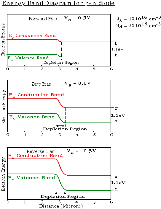
Fig. 2 The energy band diagrams for an ideal Si p-n junction diode at
three bias values. The doping densities for the p and n sides are Na =
1 x 1016 cm-3 and Nd = 5 x 1015 cm-3, respectively.
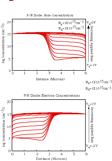
Fig. 3 Electron and hole concentration distributions for the same diode
at various biases. The doping densities for the p and n sides are Na =
5 x 1015 cm-3 and Nd = 5 x 1015cm-3, respectively.

Fig. 4 The input file to MEDICI for a typical MOS capacitor.

Fig. 5 The C-V plots at low and high frequencies for the same MOS
capacitor.
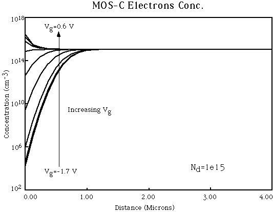
Fig. 6 Electron concentration of the MOS capacitor as a function of
distance away from the oxide layer at various bias voltages.
The n-channel MOSFET simulation is shown in Fig. 7 and 8. Fig. 7 shows
the current contour plots for a fixed gate voltage (Vg = 2 V) and
various source-drain voltages Vd. The electron concentration contour
plots are exhibited in Fig. 8 at a fixed Vd and various Vg. The 2D
contour and 3D representations provide excellent illustrations of what
actually takes place in a 3-terminal device. Without
a movie of such graphs, it takes tremendous
effort for the lecturers to explain the device behavior properly.
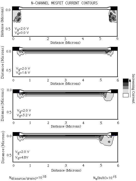
Fig. 7 Current contour plots for an n-channel MOSFET at a fixed gate
voltage (Vg = 2 V) and various source-drain voltages Vd.
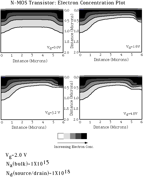
Fig. 8 Electron concentration contour plots for the same MOSFET at a
fixed Vg = 2V and various Vd.
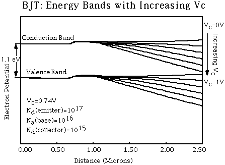
Fig. 9 Energy band diagram of an n-p-n transistor at various collector
voltages Vc and a fixed base voltage Vb.
The final example is an n-p-n transistor. The energy band diagram of
the transistor at various collector voltage Vc and a fixed base voltage
Vb is shown in Fig. 9., and vice versa in Fig. 10. The carriers can be
added on to diagrams like these to provide motion and illustration of
current flows.
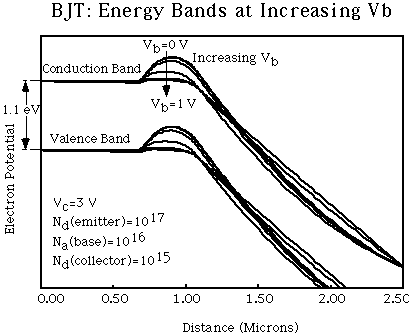
Fig. 10 Energy band diagram of the same transistor at various base
voltages Vb and a fixed base voltage Vc.
EXPECTED IMPACT AND LIMITATIONS
The use of animated simulations is expected to have a great impact in
classroom
teaching of abstract and mathematical materials. It should help to make
abstract ideas more concrete and physical. In addition, the movies will
help students to visualize time variations and spatial distributions of
various device parameters. In the next phase, we will start using the
animation as a teaching tool in the junior-level electronic devices
courses. We envision a large number of students, not only those who are
introduced to semiconductor electronics for the first time but also
graduate students and practicing engineers in the field, will benefit
from the animation videos once they are more widely used in other
courses.
One major advantage of developing the animated movies on an Apple
workstation is that Quicktime movies can be made available to students
on floppy disks. With the high accessibility to Apple computers on
campus and in the dorms, the students can play the movies at their pace
conveniently and repeatedly.
A main limitation of our methodology at present is the fact that the
animation cannot be fully interactive since the graphs are pre-generated
with a set of pre-determined device parameters and operating conditions.
This limitation is mainly dictated by the high level of computation
power required by PISCES. The device simulation thus has to be done on
a more powerful computer workstation. On the other hand, the animation
application is far more flexible and functional with Apple computers.
To overcome this limitation, we plan to make many example movies for a
variety of parameters and operating conditions so that the students can
attain a similar effect as interactive animation.
ACKNOWLEDGMENT
We acknowledge the diligent and enthusiastic work of Michael Kwong,
Danny Lee, and Keith Toh, undergraduate students in the Electrical
Engineering Department at Stanford University, who have spent their
entire summer working on all the details of this project. We express
our thanks to members of the NSF-supported National Center for
Computational Electronics (NCCE) for their help on device simulations.
Finally, we thank the generous support of the EE Department Chairs,
Professors Joe Goodman and Gene Franklin, on this project.
REFERENCES
Dutton, R. W. and Z. Yu. 1993. Technology CAD - Computer Simulation of
IC Processes and Devices. Kluwer Academic Publishers, Norwell, MA.
BIOGRAPHY
Constance Chang-Hasnain received her PhD degree in electrical
engineering from the University of California at Berkeley in 1987. From
1987 to April 1992, she was a Member of Technical Staff at Bellcore, Red
Bank, NJ. She is now an Assistant Professor and Reid and Polly
Anderson Faculty Chair in the Electrical Engineering Department at
Stanford University. Her current research include vertical cavity
surface emitting lasers, semiconductor ring lasers and Al-free
InGaAs/InGaP lasers. She has published over 45 technical journal
articles, been awarded two patents, and has contributed one book chapter.
Prof. Chang-Hasnain was awarded with the Sakrison Memorial Prize for the
most outstanding doctoral dissertation from the EECS Department at UC
Berkeley. She was named the 1991 Outstanding Young Electrical Engineer
by Eta Kappa Nu. She was awarded with the 1992 National Young
Investigator Award from the National Science
Foundation, the 1992 Packard Fellowship from the David and Lucile
Packard Foundation, and the 1993 Young Alumnus of the Year Award from
UC Davis. She is a senior member of IEEE and an elected member of
Board of Governors of the IEEE Lasers and Electro-Optics Society.
* MEDICI is a two-dimensional semiconductor device simulator developed
by Technology Modeling Associates, Inc.
** Apple's standard multimedia file format for storing sound and video
images. MacroMind uses its own format to save animations, but it can be
saved into Quicktime format.
+ An analog circuit design and simulation software developed by Beige
Bag Software.